Department of Biotechnology, Quaid-i-Azam University, Islamabad 15320, Pakistan
Commentary
A Short Note on Gold Nanoparticles
Author(s): Sumaira Anjum*
Nanoelectronics alludes to the utilization of nanotechnology in electronic parts. The term covers a different arrangement of gadgets and materials, with
the normal trademark that they are little to such an extent that between nuclear connections and quantum mechanical properties should be concentrated
widely. A portion of these up-and-comers include: crossover sub-atomic/semiconductor hardware, one-layered nanotubes/nanowires (for example silicon
nanowires or carbon nanotubes) or high level atomic hardware. Nanoelectronic gadgets have basic aspects with a size range between 1 nm and 100 nm.
Ongoing silicon MOSFET (metal-oxide-semiconductor field-impact semiconductor, or MOS semiconductor) innovation ages are now inside this system,
including 22 nanometers CMOS (correlative MOS) hubs and succeeding 14 nm, 10 nm and 7 nm FinFET (blade field-impact semiconductor) ages.. Read More»
DOI:
10.37421/2332-0796.2022.11.23
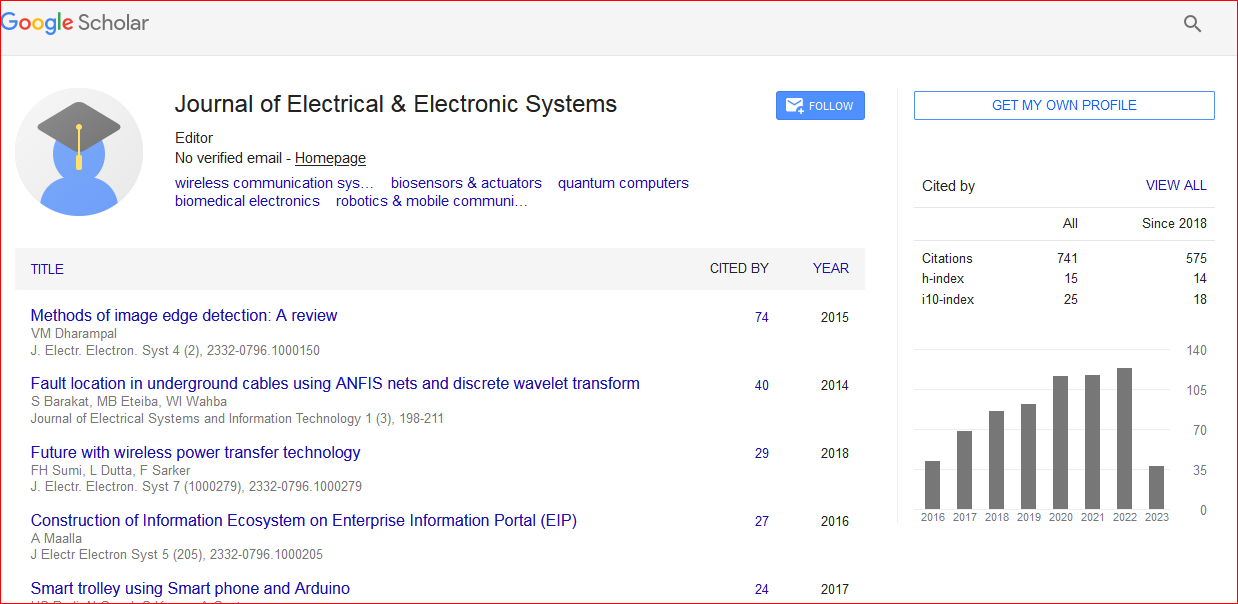
Journal of Electrical & Electronic Systems received 733 citations as per Google Scholar report

 Spanish
  Chinese
  Russian
  German
  French
  Japanese
  Portuguese
  Hindi
Hindi 