Mary M Eshaghian-Wilner, Bhuvana Bairy, T Soren Craig, Kalyani Gonde, Naman Gupta, Andrew Prajogi and Rakshith Saligram
University of Southern California, USA
Scientific Tracks Abstracts: Adv Robot Autom
Modern CMOS encounter issues altering NMOS and PMOS threshold voltages. Negative Bias Temperature Instability (NBTI) and Positive Bias Temperature Instability (PBTI) decrease drain-to-source current and increase propagation delay, due to operating temperature and stress time. NBTI also affects the timing of the circuit by varying the different propagation delays, thus vastly degrading overall performance. We therefore propose a generation-evaluation algorithm to minimize NBTI/PBTI by reducing transistor stress time through signal probability-based relative transistor repositioning. The algorithm takes a stack configuration as input and outputs the optimal configuration. For equiprobable signals, PMOS transistors connected to power supplies experience more Vth degradation than transistors indirectly connected. Therefore, the number of transistors connected to VDD in stack must be manipulated to reduce NBTI. However, assuming equal signal arrival probability is impractical. For non-equiprobable signals, the probability that a transistor is under stress is a signal probabilities function. Input degradation probability is obtained by multiplying input signal probability with the worst-case signal probability of the transistor stacked above/below depending on PMOS/NMOS, respectively. The total switching activity/equivalent stress time is the sum of each input��?s degradation probability. Given a structure, the algorithm calculates the probabilities of all possible stack configurations. The structure with smallest switching activity will undergo minimum degradation. Two configurations of an AOI logic structure under equal and unequal signal probability cases were analyzed. The preferred optimal choice is the configuration with minimal probability of being under stress.
Mary M Eshaghian-Wilner is an interdisciplinary Scientist and Patent Attorney. She is currently a Professor of Engineering Practice at the Electrical Engineering Department of USC. She is best known for her work in the areas of Optical Computing, Heterogeneous Computing, and Nanocomputing. Her current research involves the applications and implications of these and other emerging technologies in medicine and law. She has founded and/or chaired numerous IEEE conferences and organizations, and serves on the editorial board of several journals. She is the recipient of several prestigious awards, and has authored and/or edited hundreds of publications, including three books.
Email: eshaghia@usc.edu
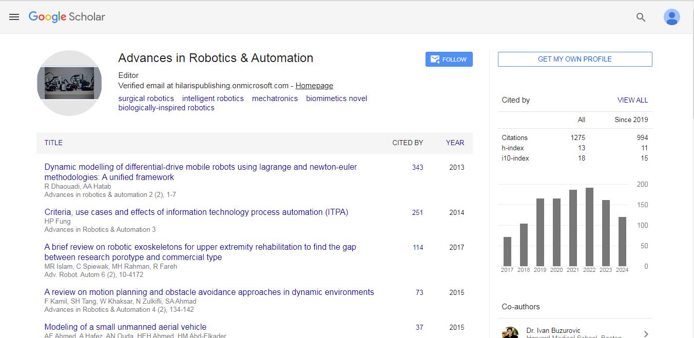
Advances in Robotics & Automation received 1275 citations as per Google Scholar report

 Spanish
  Chinese
  Russian
  German
  French
  Japanese
  Portuguese
  Hindi
Hindi 