Amitesh Kumar, Mangal Das, Brajendra S Sengar, Abhinav Kranti and Shaibal Mukherjee
Indian Institute of Technology, India
Posters & Accepted Abstracts: Adv Robot Autom
The memory effects in a memristor can be realized through the switching behavior between two distinct resistance states, low resistance state (LRS) and high resistance state (HRS) driven by low pulse voltages. ZnO-based thin films such as undoped ZnO, Mg-doped ZnO, Na-doped ZnO and Mn-doped ZnO have attracted considerable interest as promising resistive switching materials. To start with fabrication of device, 60nm thick ZnO thin film is deposited over Al/SiO2/Si substrate at a substrate temperature of 100�?°C, with DIBS background pressure of 1�?�?10-8 mBar and Ar:O2 (2:3) (flow rate in sccm), respectively. Finally, circular Al electrodes of 500�?µm is deposited on the surface of ZnO thin film. Further, I-V characteristics are measured by sweeping a DC voltage in sequence of 0-(+8 V)- 0-(-8 V)-0 in steps of 0.5V for a compliance current of 1mA. Set and reset voltages of device are evaluated to be at -6/6V. Device shows excellent endurance measured at 0.1V for 250 cycles. Retention performance assessed at 0.1V read voltage exhibits outstanding non-volatile behavior for 106s extrapolated to 10 years. Presence of oxygen vacancies (VO), interstitial oxygen ions (IO) and lattice oxygen ions are confirmed by X-ray photoelectron spectroscopy (XPS) Photoluminescence (PL) of ZnO thin film. HR-TEM image of Al/ZnO interface shows an amorphous AlOx interfacial layer (~4-5nm) formed at interface for the device in high resistance state (HRS) state. Formation of this interfacial layer at RESET voltage transits the device from LRS to HRS and dissolution at SET voltage leads to change device state to LRS. Our memory device as fabricated by DIBS exhibits excellent performance parameters, retention and endurance to implement it for a practical RRAM. Our work could play a very significant role in realizing similar memristive devices with high performance parameters in future. phd1401102005@iiti.ac.in
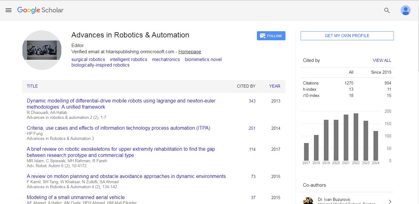
Advances in Robotics & Automation received 1275 citations as per Google Scholar report

 Spanish
  Chinese
  Russian
  German
  French
  Japanese
  Portuguese
  Hindi
Hindi 