Brief Report - (2022) Volume 10, Issue 6
Received: 03-Jun-2022, Manuscript No. jaat-22-68570;
Editor assigned: 05-Jun-2022, Pre QC No. P- 68570;
Reviewed: 17-Jun-2022, QC No. Q- 68570;
Revised: 21-Jun-2022, Manuscript No. R- 68570;
Published:
29-Jun-2022
, DOI: 10.37421/ 2329-6542.2022.10.218
Citation: Kociak, Mathieu. “Schematic of a STEM Fitted with an
EELS Spectrometer and a CL Identification Framework.” J Astrophys Aerospace
Technol 10 (2022): 218.
Copyright: © 2022 Kociak M. This is an open-access article distributed under the
terms of the Creative Commons Attribution License, which permits unrestricted
use, distribution, and reproduction in any medium, provided the original author
and source are credited.
Lately, the quantity of investigations on the optical properties of nanoparticles or nanostructured materials has in a real sense detonated. Most presumably, this is because of the way that these optical properties can be controlled and planned freely by playing with the nanostructures sizes and shapes, and the abilities and imagination of scientists and technologists have given throughout the last years the physicist with an admittance to such deliberately planned Nano-objects [1]. These days, the significant scale can be pretty much as little as a nanometer for optical properties and, since these are so subject to the construction and morphology, these last option might need to be known with a nuclear accuracy [2].
For sure, numerous key and more applied issues depend on the perception of optical properties at these scales. For instance, the way of behaving of the light at distances a lot more modest than its frequency is an entrancing and illogical subject [3]. One more model is the improvement of Light Emitting Diodes (LEDs), or the advancement of photovoltaic gadgets, that intensely depend on the scaling down and Nano structuration of the materials they are comprised of. It is hence an astonishing test to investigate and quantify the optical properties varieties of such significant modern gadgets at the important scale, for example more than a couple of nanometres scale. Consequently, the central furthest reaches of optical procedures depending on photons alone require the presentation of troublesome techniques and ideas, which have seemed these last years and which will be depicted in this survey paper [4].
Obviously, standard optical means, for example, noticeable UV spectroscopy or Photoluminescence, P, even in a confocal set-up, can't go beneath as far as possible and can't resolve the issue effectively. Staggering optical procedures, like the STimulated Emission Depletion (STED), can now arrive at genuine nanometer goal, alternatively in 3D. Notwithstanding, they are restricted to explicit applications, and can't help at deciding the design or morphology of the objects of interest. Different other options, like the Photoemission Electron Microscopy (PEEM) regardless of their advantage, have not yet shown goals better than a couple of nanometres [5].In an EELS try, a quick electron shaft is sent onto the example of interest, and the inelastically dissipated electrons are shipped off a scintillator in the wake of having been scattered in energy through an attractive crystal.
The EELS range is in this way imaged onto a (these days) CCD camera because of a coupling optics. An EELS range, by and large comprises in the accompanying parts: an extraordinary pinnacle, called "zero-misfortune top" (ZLP) in light of the fact that it contains just electrons that poor person in elastically cooperated with the example in a quantifiable manner, trailed by the purported low misfortune district (from commonly 0.5 to 100 eV), and the center misfortune locale (from regularly 100 eV to a few keV). The last option contains significant data about the science, valence, holding state and all the more by and large the electronic construction and is currently a far reaching procedure that can gather such a data down to the single nuclear section. In the accompanying, just the IR/VIS/UV a piece of the range is thought of. It is quite important that this reach compares to an exceptionally confined piece of the enormous elements in an ordinary EELS range.
The authors declare that there is no conflict of interest associated with this manuscript.
Google Scholar, Crossref, Indexed at
Google Scholar, Crossref, Indexed at
Google Scholar, Crossref, Indexed at
Google Scholar, Crossref, Indexed at
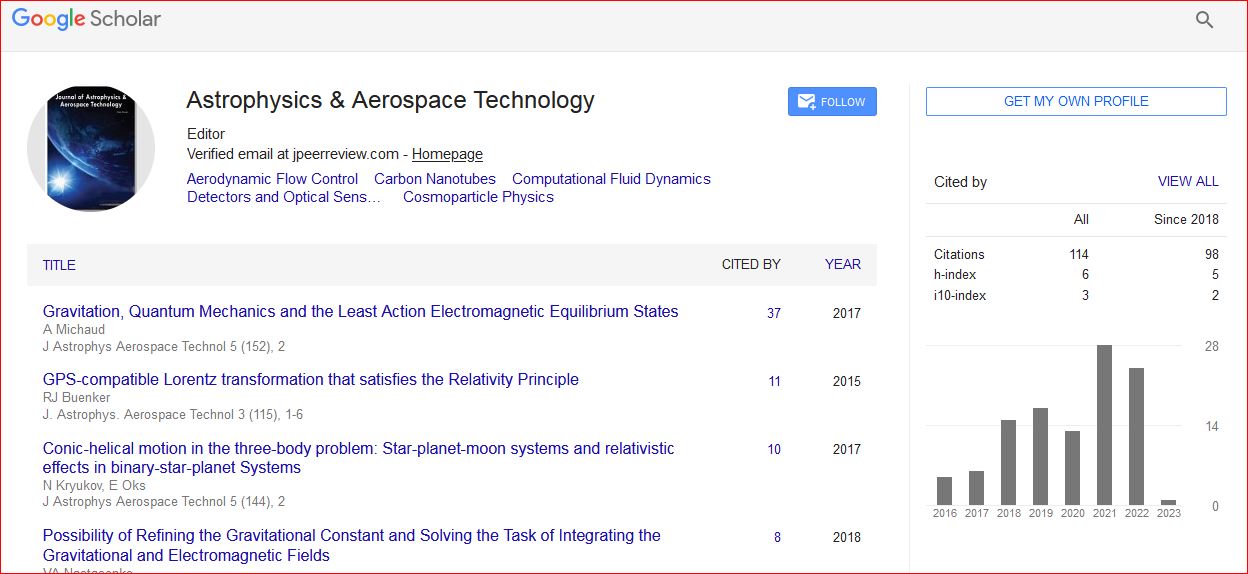
Astrophysics & Aerospace Technology received 114 citations as per Google Scholar report