P. Yadav
Trinity College Dublin, Dublin, Ireland
Scientific Tracks Abstracts: Bioceram Dev Appl
In recent years, miniaturisation of integrated circuit (ICs) and the demand towards increased 3D functionality have led to integration complexity. To meet the fabrication challenges of next generation electronic devices, novel materials and new processing methods are required. In particular, area selective deposition (ASD) approaches have gained much interest as a way to produce direct deposition of the desired material while reducing processing step(1). Critical to this are molecular systems that have selective surface binding and can act as the template to the material growth or surface deactivation. Our recent work we demonstrate grafting of end functionalised polystyrene, polymethylmethacrylate, and poly-2(vinyl pyridine) as templates to produce highly coherent oxide films(2). A facile approach for rapid grafting (in seconds) of polymer brush films with complete coverage over large area with high uniformity is shown (pinhole free). The influence of the molecular weight, solution concentration of the polymer, solvent selectivity, process time and temperature on the final film formation (Figure 1). Exposing the covalently grafted polymer brush (P2VP-OH) to a metal salt-solvent solution (using the Al3+ions) swells the polymer, facilitating ion inclusion. X-ray photoelectron spectroscopic analyses reveal that the infiltration of several other metal such as Hf+4, Zr+4, Ti+4 and Ru+3to the polymer brush film. Early results suggest a solvent mediated approach to polymer film infiltration can be used to develop inorganic film in facile approach. Whilst data shows inclusion in to large area and pattered films, the mechanism and understanding of these has been limited. Solution mediated process described in our studies shows the precise tailoring of nanometre thin polymer films that are pinhole free that can be activated to create semiconductor compatible oxide films that are parallel in quality to ALD or CVD derived process.
I obtained a Master of Science qualification in organic chemistry from University of Mumbai in 2015 and then spent two years in the Indian Institute of Technology Mandi undertaking research in photoresist synthesis and characterisation. In May 2018, I joined the lab of Prof. Morris as a PhD candidate in Trinity College Dublin researching Area Selective Deposition (ASD) technologies. ASD is an emerging technique for self-aligned deposition of materials and a viable candidate to compliment established semiconductor nanofabrication processes. Placing inorganic materials, and in particular oxides and metals is imperative in 3D integration of near and long-term memory and logic demands for nanoelectronic fabrication.
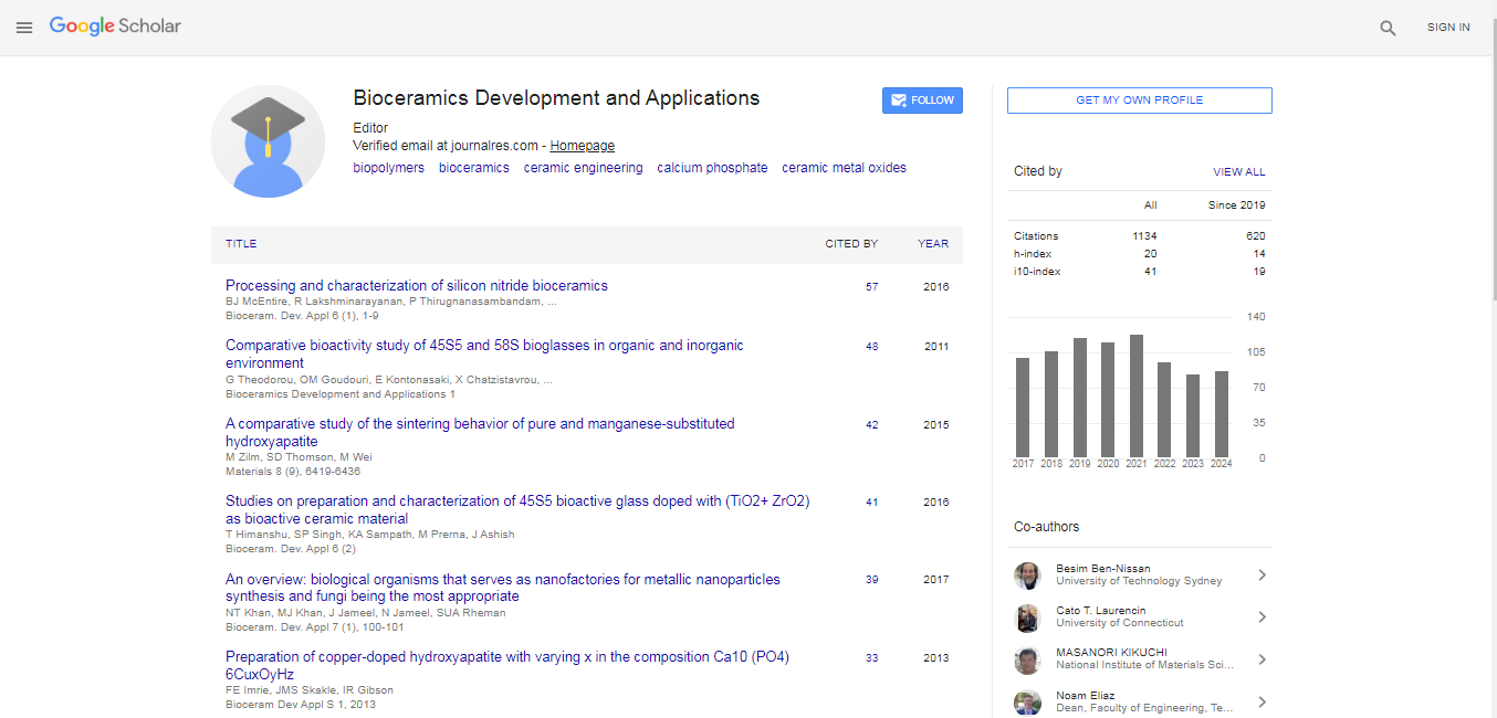
Bioceramics Development and Applications received 1050 citations as per Google Scholar report

 Spanish
  Chinese
  Russian
  German
  French
  Japanese
  Portuguese
  Hindi
Hindi 